
Closing the Gap to E-Beam: The DWL 66+ Now Delivers 200 nm Features and Unrivaled Grayscale
- rocheller44
- Jul 22, 2025
- 2 min read

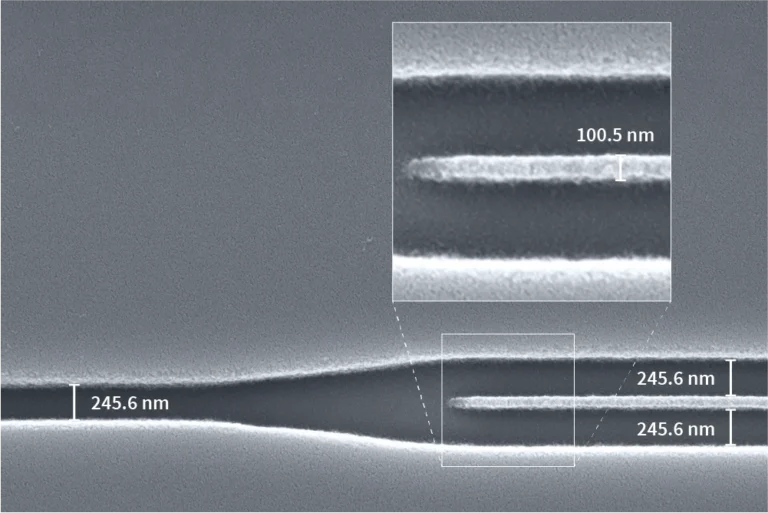
The 200 nm Frontier: Bridging the Gap to E-Beam
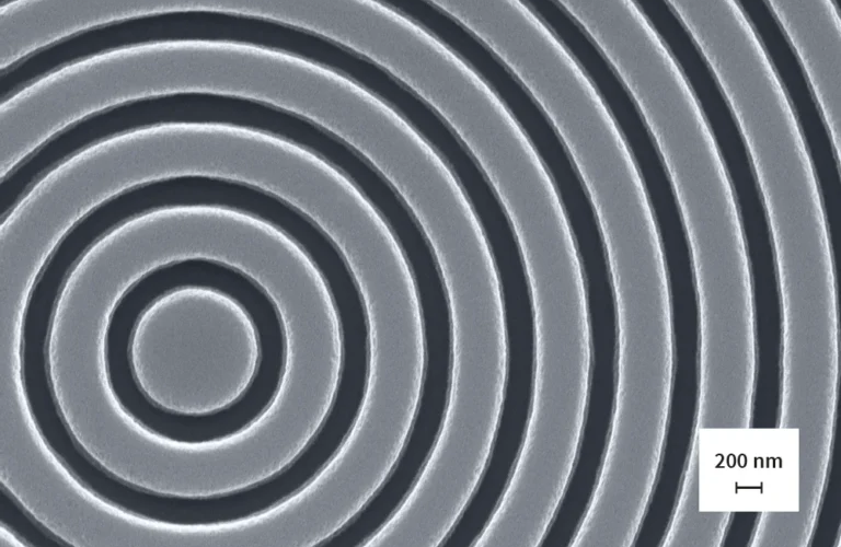
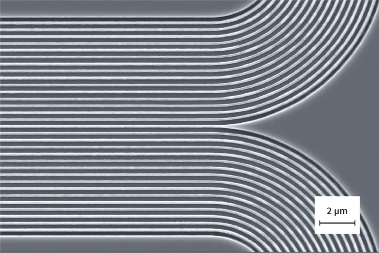
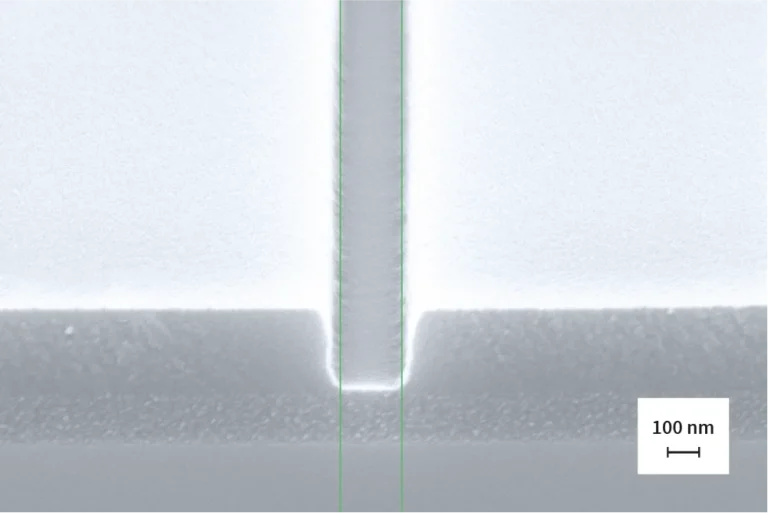
For the most demanding applications in photonics, microelectronics, and quantum devices, achieving the smallest possible feature size is paramount. With the new Write Mode XR, the DWL 66+ now delivers a minimum feature size of 200 nm—the highest resolution of any direct-write laser system on the market.
This breakthrough means you can now:
Fabricate finer, more complex structures than ever before.
Handle tasks previously exclusive to costly e-beam lithography.
Dramatically accelerate your development cycles and optimize your lab’s workflow.
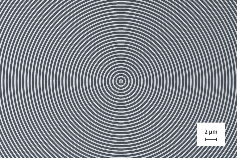
The Power of the Third Dimension: 65,536 Shades of Gray
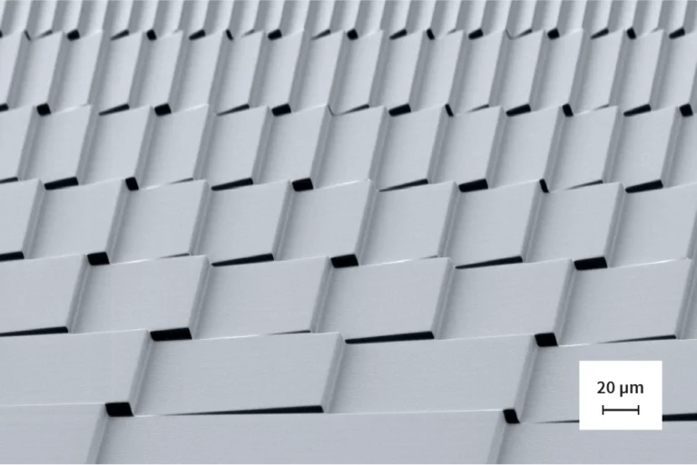
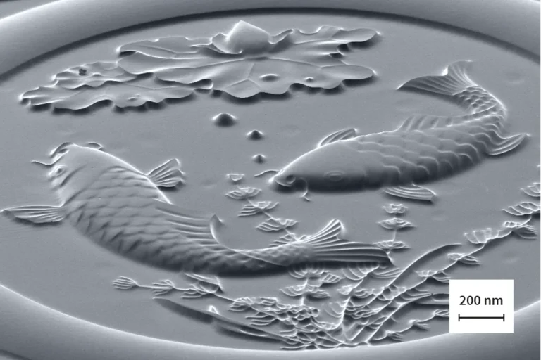
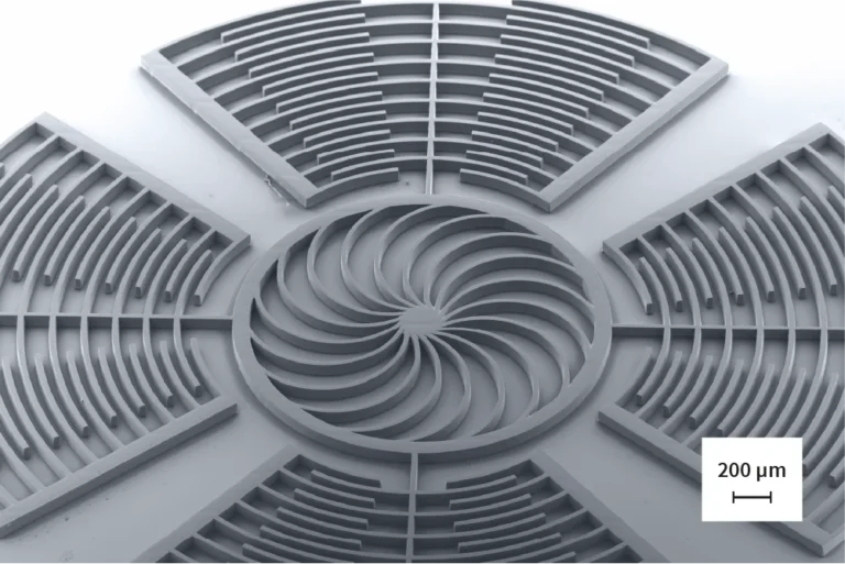
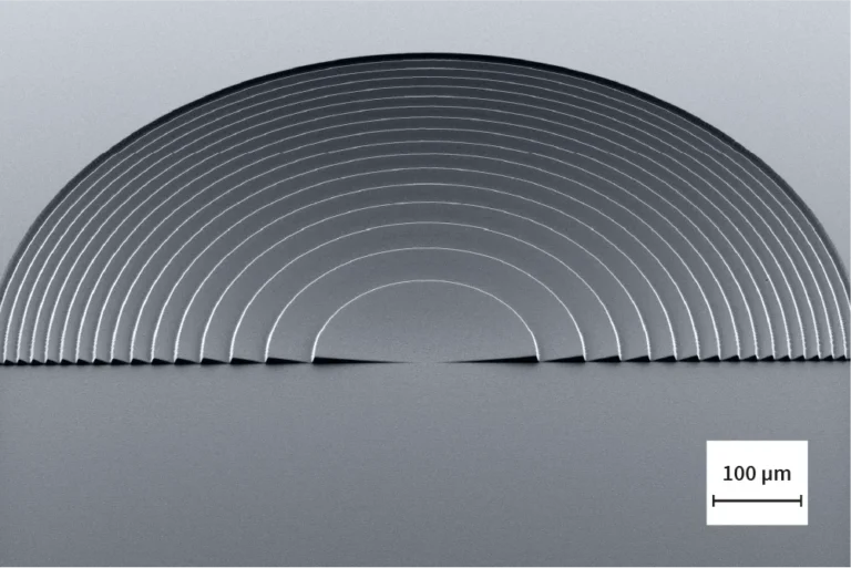
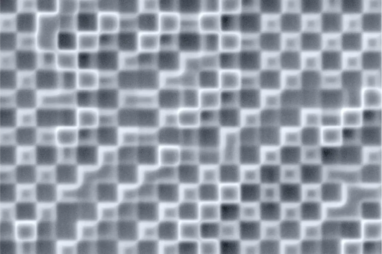
Modern microfabrication is about more than just 2D patterns. The ability to create complex, smooth, three-dimensional surfaces is critical.
The enhanced DWL 66+ masters this challenge with its professional-grade grayscale capability, now offering an unprecedented 65,536 distinct exposure levels. This incredible precision allows you to fabricate intricate 2.5D topographies, such as micro-lenses or blazed gratings, with outstanding surface quality, even in resists up to 150 µm thick. This is the finesse you need to shape light with micro-optics or engineer complex micro-electronics.
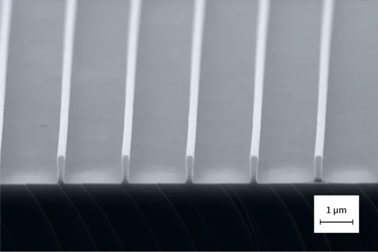
Flexibility for Real-World Research
These new features are built upon the proven flexibility of the DWL 66+ platform. As a maskless system, it enables instant design changes and rapid prototyping, eliminating costly mask-related delays. It handles virtually any substrate—flat, curved, standard, or exotic.
This isn’t just an upgrade; it’s a gateway to new possibilities in optics, photonics, quantum devices, and beyond.


Contact us today for more information.


Comments