Quantum Computing
-
All in one quantum control stack solution for controlling superconducting qubits
-
Modular approach with signal generation & acquisitian up to 18.5GHz
-
Scalable to >1000 qubits
Qblox offers fully integrated quantum control stacks designed specifically for controlling and reading out spin qubits in various materials such as GaAs, Si, or Ge quantum dots.
Qblox quantum control stack, the Cluster, integrates electronics and software needed for optical setups to control and readout NV centers and trapped ions. This integrated solution streamlines experiments and finds applications in quantum sensing, computing, and communication.
-
ALD of Superconducting NbN for Single Photon Detectors
-
Silicon/SiNx Etch for Low-loss Optical Components
-
PE/ICPCVD of Si3N4 for Low-loss Optical Components
-
Atomic Layer Deposition of Superconducting TiN
-
Atomic Layer Deposition of Superconducting NbN
-
Plasma Etching of Superconducting Metals and Nitrides
-
Atomic Layer Deposition of Tunnel Barriers
-
Deep Silicon Etch (DSiE) for TSV
-
Plasma Etching of Diamond with NV Centres
-
Plasma Etching for Creating Efficient Light Coupling Components
-
Heidelberg Instruments offers a comprehensive portfolio of tools to manufacture various structures crucial for quantum devices to revolutionize computing, sensing, and data communication.
-
NanoFrazor systems, renowned for ultra-high resolution capabilities which allow for precise fabrication, minimizing damage and a bridge to future production.
-
DWL series enables the creation of 2.5D topographies.
-
VPG+ produces high-precision masks suitable for mass manufacturing.
-
MPO 100 tool is designed for manufacturing 3D micro-structures.
-
Maskless Aligners (MLA) are ideal for multi-layer device fabrication.
Below a certain size, the quantized structure in nanoparticles becomes visible. So called quantum well structures are formed, with special electronic properties. ARPES is a powerful tool to characterize the quantum electronic structure.
QUBITS are the smallest functional unit of a quantum information processing device or, in other words, a quantum computer. The electronic transport properties can be probed by a Nanonis Tramea system connected to a low temperture cryostat.
-
Die Bonding placing microchips
-
Wedge-Wedge wedge-bonding with 25µm gold wire
-
Ball-Wedge ball-bonding with 25µm gold wire
-
Ribbon bonding with ribbon
-
Bumps bump-bonding in flip-chip applications
-
Heavy Wire bonding wire from 100μm to 500μm
-
Battery bonding battery packs
-
Copper bonding with copper wire
-
Coated bonding aluminum coated copper wire
-
Insulated bonding insulated wires over soldering
Atmospheric pressure plasma is used in wire bonding as a selective fine cleaning step to remove contamination and residues from the contact surfaces. In general, strong bonds between wire and substrate can only be achieved on clean contact surfaces (bond pads). Thus, plasma treatment has a considerable effect on the quality and consequently the reliability of the entire component.
Accessing qubits and making these remarkable devices communicate with the outside world requires the fabrication of high-resolution electrodes as well as larger structures such as electrical wiring and contact pads. With the NanoFrazor NextGeneration tool with Mix & Match patterning capabilities to combine the best of t-SPL and DLS all within one tool with one software and one film stack.
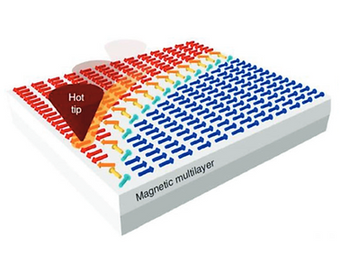
Manipulating the spin orientations of electrons in thin films by thermally adjusting the crystal structure at sub-100 nm resolution is possible with the NanoFrazor. Thermal stimulus from the t-SPL module can be used for the high-temperature manipulation for spintronic applications, as well as local changes to magnetic states and even triggering of phase transitions.


