


DWL 66+
The ultimate lithography research tool
The DWL 66+ delivers unrivaled versatility, professional-grade grayscale capabilities, and the highest resolution of any direct-write laser system on the market.
As a highly versatile system, the DWL 66+ is designed for R&D and rapid prototyping in MEMS, microelectronics, microfluidics, sensors, optics, photonics, photovoltaics, material sciences, quantum devices — virtually any application that requires microstructure fabrication.
Key Features
High-Resolution Mode with 200 nm Minimum Feature Size: Our Write Mode XR delivers an unsurpassed combination of resolution, quality, and speed.
Grayscale Exposures with 65,536 Levels: Enabling grayscale exposures with outstanding surface quality in resists of up to 150 µm thickness.
Fully Customizable System Configuration: 30 years of continuous development and over 400 installed units make the DWL 66+ the most versatile and proven system on the market.
Take your Optimal Lithography to a New Level
The DWL 66+ is not just a replacement for your mask aligner : It is an upgrade that offers a new level of accuracy, resolution, and structure fidelity. This maskless system will drastically reduce the time needed to develop new devices and it will offer new possibilities.
Instant Design Changes: Modify your CAD file and begin exposing immediately. No mask-related costs, effort, waiting time, or security risks.
Diverse Substrate Compatibility: The DWL 66+ exposes not only on standard chips or wafers, but on substrates of any material, size, thickness or shape – including curved surfaces.

Reduce the workload of your e-Beam Lithography System: In many cases, the DWL 66+ can perform exposures previously requiring an e-beam lithography system, freeing your e-beam for more demanding tasks.
Uncompromising Exposure Quality
The DWL 66+ is engineered for R&D, yet it incorporates core technologies from our industrial production systems to ensure the highest level of accuracy and reproducibility.
Controlled Environment: The DWL 66+ system includes a laminar flow box to minimize particle contamination and ensure thermal stability during exposures.
Interferometric Position Control: A high-resolution interferometer in combination with a real-time beam position correction ensures pattern placement accuracy and structure fidelity.

Real-time Autofocus System: The DWL 66+ includes the common optical autofocus system, but is enhanced by a proprietary secondary autofocus system that functions independently of optical feedback. This enables precise focusing even on transparent or low-reflectivity substrates.
Optimized Combination of Quality and Productivity
The DWL 66+ does not compromise on exposure quality to increase throughput. The write speed is specified for the highest quality setting and the write time will not depend on fill factor, shape, or number of structures within the exposure area.
Exchangeable Write Modes: Easily switch between Write Modes to optimize resolution and throughput for your application.
Proprietary Software and Hardware: The intuitive user interface, combined with optimized design preparation and fast data conversion, enables a rapid workflow from setup to exposure.
Full Automation: The operation of the DWL 66+ can be fully automated with automatic front- or back side alignment and a cassette-to-cassette handling system.
>400
Installed Systems
Customer applications
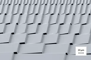
Blazed Gratings at various angles from 10 to 70 degrees.

DWL 66+ exposure of concentric rings with a linewidth of approximately 200 nm and a pitch of 700 nm in positive photoresist.

Pushing the limits with Write Mode XR – lines and spaces with 400 nm pitch.

Why customers choose our systems
"Ordering a DWL 66+ machine during the time of the Corona pandemic was a great challenge. It turned into an advantage. Installation was in time. By remote training, we learned quickly about grayscale lithography, developed basic process knowledge with the help of three bachelor students, and jumped into our first industrial projects that gave us real-life experience and insight into the capability of our new tool. During this time, we had an intensive exchange with Heidelberg Instruments that was instrumental to go beyond the basics of 3D lithography. It is therefore easy to say that choosing the DWL 66+ was the right thing to do, and it complements well the other lithography techniques that we pursue at Paul Scherrer Institute."
Dr. Helmut Schift, Head of Advanced Nano Manufacturing Group
Paul Scherrer Institute (PSI),Villigen, Switzerland
Technical Data
Write Mode | XR | I | II | III | IV | V |
|---|---|---|---|---|---|---|
Minimum Feature Size [μm] | 0.2 | 0.6 | 0.8 | 1 | 2 | 4 |
Minimum Lines and Spaces [μm] | 0.3 | 0.8 | 1 | 1.5 | 3 | 5 |
Address Grid [nm] | 5 | 10 | 25 | 50 | 100 | 200 |
Edge Roughness [nm] | 50 | 50 | 70 | 80 | 110 | 160 |
CD Uniformity [nm] | 60 | 70 | 80 | 130 | 250 | 400 |
2nd Layer Alignment over 5 x 5 mm² [nm] | 250 | 250 | 250 | 250 | 350 | 500 |
2nd Layer Alignment over 100 x 100 mm² [nm] | 500 | 500 | 500 | 500 | 800 | 1000 |
Backside Alignment [nm] | 1000 | 1000 | 1000 | 1000 | 1000 | 1000 |
Write Speed [mm²/min] with Diode Laser (405 nm) | 3 | 13 | 40 | 150 | 600 | 2000 |
Write Speed [mm²/min] with UV Diode Laser (375 nm) | 2 | 10 | 30 | 110 | - | - |
Pixel Grid in x and y [nm] | 50 | 100 | 250 | 500 | 1000 | 2000 |
Scan Speed [mm/s] | 1800 | 3600 | 4500 | 9000 | 18000 | 36000 |
System Features | -- |
|---|---|
Light Source | Diode laser with 405 nm or 375 nm |
Substrate Sizes | Variable: 5 x 5 mm² to 9″ x 9″ | Customizable on request |
Substrate Thickness | 0 to 12 mm |
Maximum Exposure Area | 200 x 200 mm² |
Environmental Chamber | Temperature stability ± 0.1°, ISO 4 environment |
Real-Time Autofocus | Optical autofocus or air-gauge autofocus |
Autofocus Compensation Range | 80 μm |
Standard or Advanced Grayscale Mode | 128 or 32,768 gray levels respectively |
Vector Mode | Enables the writing of stitching-free lines |
Overview Camera | 13 x 10 mm² field of view facilitates alignment to marks and substrate navigation |
Backside Alignment (optional) | Allows the alignment of exposures to structures on the backside of the substrate |
Advanced Options - Performance Upgrades | -- |
|---|---|
Automatic Loading System | Handling of masks up to 7" and wafers up to 8" with two carrier stations, pre-aligner and wafer scanner |
Professional Grayscale Mode | 65,536 gray levels, professional data conversion software |
High-Accuracy Coordinate System | Includes golden plate calibration and climate monitoring: 2nd layer alignment over 100 x 100 mm² improved to 350 nm |
System Dimensions of Standard Version | -- |
|---|---|
Width × depth × height | 1300 mm × 1100 mm × 1950 mm (lithography unit only) |
Weight | 1000 kg (lithography unit only) |
Installation requirements | -- |
|---|---|
Electrical | 230 VAC ± 5 %, 50/60 Hz, 16 A |
Compressed air | 6 - 10 bar |
